
The Semiconductor Industry Future: Navigating Innovation with Intelligence
Imagine this: You’re a young process engineer at a semiconductor fabrication plant, and today a yield loss investigation has been escalated to your team. A subtle yet persistent defect is lowering wafer yields despite stable equipment and materials. As you dig into defect analytics aided by AI-powered simulations, you realize this is a moment for blending experience with emerging technologies—a situation that perfectly illustrates where the semiconductor industry is headed.
In this Omnivance Premium Editorial, we explore the semiconductor industry's future, providing a strategic outlook grounded in industry intelligence. Designed for students and working professionals alike, this feature builds practical, long-term professional capability in a sector crucial to powering the modern digital economy.
The Semiconductor Industry’s Strategic Role in Tomorrow’s Digital World
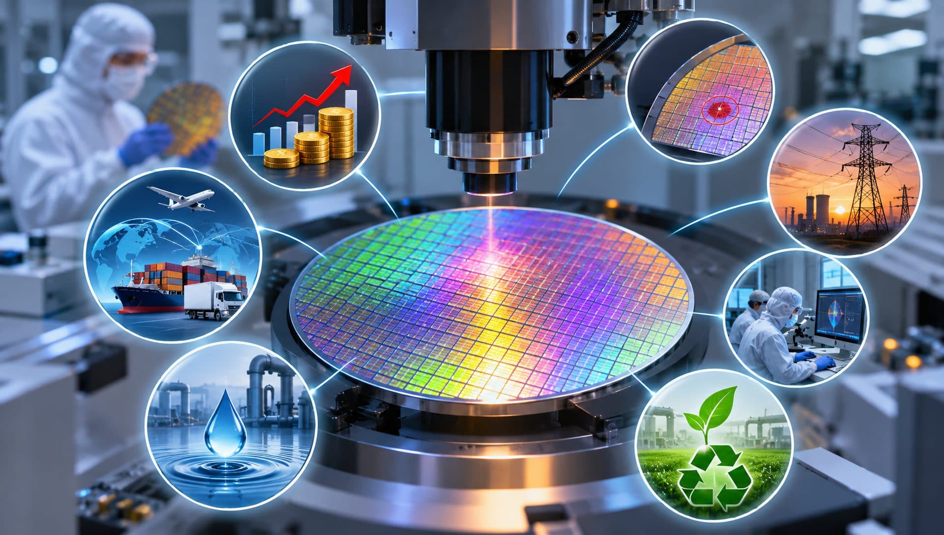
The semiconductor industry touches every facet of modern life, from smartphones to smart grids, autonomous vehicles to cloud computing infrastructure. As part of a larger ecosystem—the digital economy—it functions as a strategic enabling industry that designs, fabricates, and delivers the “brains” of digital innovation.
At the core lies the semiconductor value chain, spanning architecture, design, verification, fabrication, packaging, testing, and ultimately, delivery to customers. Each segment involves specialized roles—design engineers, verification teams, process and test professionals, equipment specialists, quality assurance, product managers, and supply chain experts. Together, they uphold stringent business principles of precision, reliability, yield economics, speed to market, and close collaboration.
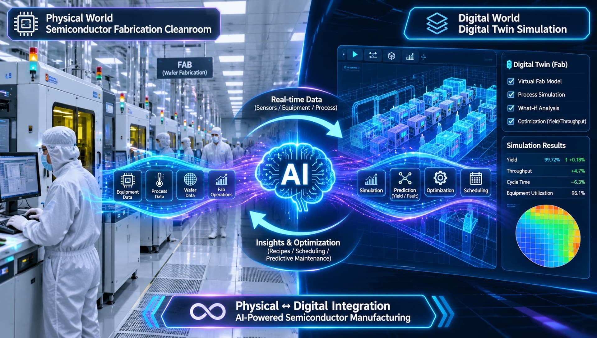
Looking ahead, the industry is evolving rapidly, driven by technological advancements and shifting market demands. The future will be shaped by innovations such as chiplets (modular chip components), AI-optimized processors, digital twin simulations of fabs, and smart fabs powered by real-time analytics—all intersecting with AI and advanced manufacturing technologies.
Why Should You Care About the Industry’s Future?
You might ask: *Why should I invest effort learning about the future of an industry known for cutting-edge complexities and relentless innovation?* Whether you’re a graduate entering your first semiconductor design internship or a quality manager overseeing packaging reliability, understanding industry trends is essential to grow beyond day-to-day tasks into impactful roles.
Consider a scenario: an experienced test engineer uses predictive maintenance tools to foresee equipment downtime before it happens. This proactive approach, enabled by AI and metrology advances, reduces yield losses and aligns production schedules tightly with market demands. Such intelligent application of emerging technologies transforms challenges into competitive advantage.
In essence, mastering the future means enhancing your professional judgment with new tools, continuously improving your problem-solving capabilities, and proactively contributing to innovation cycles. It’s not about chasing certifications or immediate pay raises but building resilient, adaptable expertise that ensures career longevity and organizational success.
Key Technologies Shaping the Semiconductor Industry Future
1. Chiplets and Modular Architecture
Traditional monolithic chips are giving way to modular chiplets—smaller, specialized functional blocks that manufacturers assemble into complex systems. This shift improves design flexibility, reduces costs, accelerates development, and addresses yield challenges by isolating defects to individual chiplets.
*Workplace example:* A design engineer participating in a chiplet integration review must collaborate closely with the verification team and packaging specialists to ensure interconnect standards and reliability targets are met, avoiding late-stage redesigns that can delay delivery.
2. AI-Driven Defect Analytics and Yield Improvement
Yield—the proportion of wafers or chips that meet quality standards—is a critical economic parameter. Employing AI to analyze defect patterns, process variations, and equipment performance enables early detection of yield degradation causes.
*Workplace example:* During a yield loss investigation, AI tools aggregate data across metrology instruments and lithography equipment to identify nuanced correlations invisible to manual inspection, enabling faster root cause analysis and corrective action.
3. Digital Twins and Smart Fabs
Digital twins are precise virtual replicas of semiconductor fabs that simulate processes in real time, enabling predictive modeling, process optimization, and what-if scenario analysis without interrupting physical operations.
*Workplace example:* A process engineer uses a digital twin to simulate the impact of changing lithography exposure parameters on wafer uniformity, collaborating with equipment engineers to refine settings that improve yield without risking production continuity.
4. Advanced Packaging and 3D Integration
As nodes shrink, packaging technologies evolve beyond simple protection and signal routing—3D stacking and heterogeneous integration address performance bottlenecks and power efficiency by bringing components closer together.
*Workplace example:* A packaging quality professional works with the design and test teams to validate thermal management solutions in stacked chip modules, ensuring reliability under real-world operating conditions.
Business Impact of Embracing Industry Future Trends
The semiconductor industry’s future hinges on balancing speed to market with precision and reliability. Innovations such as AI-assisted defect detection accelerate problem solving, reducing costly downtime. The modular chiplet approach shortens design cycles and enhances scalability. Digital twins optimize fab performance, boosting yield and resource utilization.
For companies, the implications are profound: improved customer satisfaction from higher-quality products, reduced production costs through better yield economics, and greater market agility. This creates a virtuous cycle of innovation that promotes sustained competitiveness amid global supply chain complexities and geopolitical uncertainties.
From a career perspective, professionals equipped with knowledge of these technologies and collaborative skills—working across R&D, fab operations, and customer engagement—become invaluable contributors and problem solvers. Their ability to integrate AI insights with domain expertise derives business value beyond routine job functions.
Collaboration as the Cornerstone of Future Success
No semiconductor innovation happens in isolation. Collaboration is the strategic glue that binds cross-functional teams, suppliers, customers, and even academic partners. The complex value chain necessitates transparent communication and joint problem solving, especially when integrating chiplets, aligning AI models with fab data, or qualifying new packaging technologies.
At an organizational level, cross-team efforts like design reviews that incorporate verification, process, and test feedback foster faster issue resolutions, while supplier partnerships that share metrology data enable predictive maintenance strategies.
In practice, professionals should proactively develop collaboration capabilities: active listening, interdisciplinary language fluency, and digital tools proficiency to bridge diverse functional perspectives and accelerate knowledge sharing.
Building Your Career for the Semiconductor Industry Future
Entering or advancing in the semiconductor industry today means embracing a growth mindset built on three pillars:
Capability before compensation: Focus on mastering problem-solving in yield loss investigations or design optimizations, rather than short-term salary gains.
Learning before certification: Prioritize hands-on exposure to AI tools, digital twin platforms, or lithography process improvements over accumulating certificates.
Growth before promotion: Seek experiences that build cross-functional leadership, such as participating in multi-team collaboration on chiplet integration.
Consider this framework for professional growth:
Growth Dimension | Practical Focus | Example Activity |
Technical Mastery | Understanding emerging tech | Learn AI-driven defect analytics platforms |
Cross-functional Skills | Collaboration and communication | Lead design-verification-process meetings |
Strategic Thinking | Aligning innovations with business goals | Participate in product roadmap discussions |
Adaptability | Embracing change and rapid learning | Support deployment of digital twin simulations |
Cultivating these attributes not only enhances day-to-day impact but also prepares you to navigate the evolving industry landscape.
Takeaway and Reflection
The semiconductor industry’s future is a dynamic interplay of advanced technologies, intelligent processes, and collaborative ecosystems. Its strategic role in the digital economy ensures ongoing innovation that demands both technical mastery and adaptive professional growth.
Reflect on your current role or studies: How are you integrating new technologies and cross-functional collaboration to solve problems smarter and faster? What steps can you take this month to deepen your understanding of AI applications or digital twin simulations in your work or learning environment?
As you contemplate these questions, prepare to explore our next topic: AI in Semiconductor Verification: Enhancing Precision and Speed, where we delve deeper into how AI tools are revolutionizing design verification workflows.
Frequently Asked Questions
What is the semiconductor value chain, and why is it important?
The semiconductor value chain encompasses the stages from architecture and design to fabrication, packaging, testing, and delivery to customers. Each step requires specialized skills and technologies. Understanding this chain is crucial because it highlights where innovations and improvements—such as AI analytics or advanced packaging—can increase yield, lower costs, and accelerate time to market.
How do chiplets differ from traditional monolithic chips?
Chiplets are smaller, modular blocks of silicon that designers assemble into single-chip systems, contrasting with traditional large, monolithic chips. This approach enhances design flexibility, improves yields by isolating defects, and reduces development times by enabling reuse of proven blocks. It’s a major trend reducing complexity and cost in next-generation semiconductors.
How is AI practically used in semiconductor manufacturing today?
AI algorithms analyze vast amounts of metrology and equipment data to detect defect patterns, predict equipment failures, and optimize process parameters. For example, AI-driven defect analytics can quickly pinpoint root causes of yield loss, enabling engineers to fix problems before they escalate, thereby saving time and resources.
What collaborative skills are most valuable in the semiconductor industry?
Key skills include effective communication across disciplines, active problem-solving with input from design, process, test, and supply chain teams, and digital fluency for sharing data insights. These skills enable smoother cross-functional collaboration essential for innovations like chiplet integration and digital twin usage.
How can early-career professionals develop capabilities aligned with industry future trends?
They should seek hands-on exposure to emerging tools such as simulation platforms and AI analytics, participate actively in design and yield review processes, and cultivate interdisciplinary communication skills. Prioritizing real-world learning over certification helps build deep expertise needed for long-term growth.
What are digital twins, and what future developments might they enable?
Digital twins are high-fidelity virtual models of semiconductor fabs replicating physical processes in real time. They enable predictive optimization without interrupting production. Future developments may include fully autonomous fabs that self-adjust parameters dynamically or advanced scenario planning to accelerate new technology introduction.
Explore next: AI in Semiconductor Verification: Enhancing Precision and Speed
Embark on deeper learning about how AI-supported verification is transforming design reliability and speeding innovation cycles, reinforcing your strategic positioning in the semiconductor industry’s evolving future.
Tags
Share this article

Omnivance Research Team
Dedicated to bridging the gap between education and industry requirements.
Related Courses
Deepen your knowledge with these recommended courses