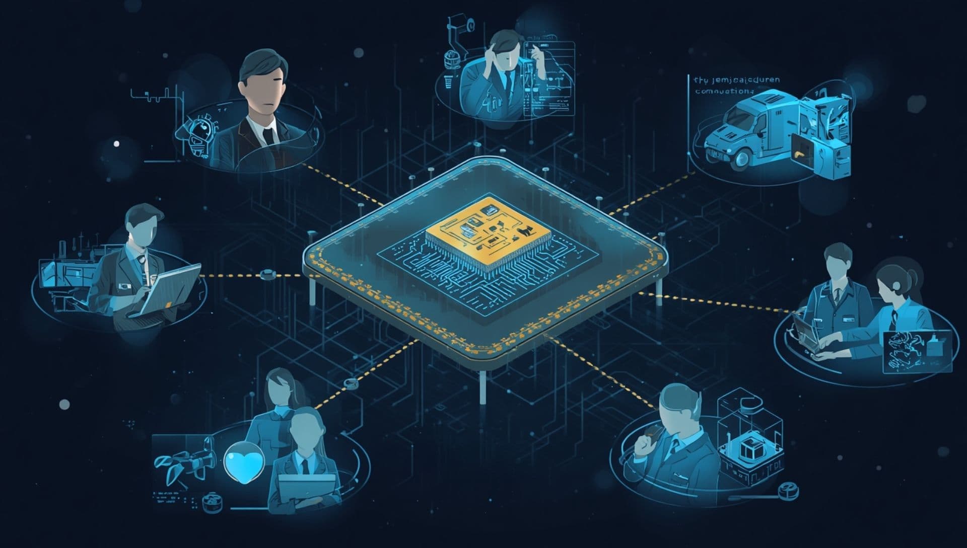

Imagine you’ve just joined a semiconductor company as a junior engineer or supply chain analyst. You attend your first cross-functional meeting where team members from design, fabrication, and testing are debating a production delay. As someone new, you want to understand how all these pieces connect—who does what, why each step matters, and how your role fits into the bigger picture. That’s the essence of grasping the semiconductor industry value chain.
Understanding the Semiconductor Value Chain: More Than Just Chips
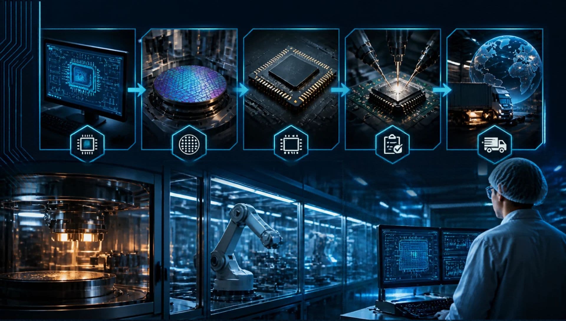
Semiconductors power nearly every modern digital device—from smartphones and data centers to cars and healthcare equipment. But making these tiny silicon chips involves a highly specialized, multi-step process that stretches from early concept to customer delivery. The semiconductor value chain comprises seven major stages:
- Architecture: Defining the chip’s fundamental functions and system integration
- Design: Building detailed circuit schematics and layouts using Electronic Design Automation (EDA) tools
- Verification: Testing designs virtually to ensure correctness before manufacturing
- Fabrication: Using photolithography and chemical processes to produce the silicon wafers
- Packaging: Encasing the silicon die for protection and connectivity, increasingly involving advanced packaging technologies
- Testing: Electric and functional testing at wafer and packaged chip level to guarantee quality and yield
- Customers: Supplying the final chips to device manufacturers and end users along with qualification and support
Each of these stages is a critical business function, with specific professional roles and challenges. Precision, reliability, speed to market, and collaboration underpin success from end to end.
What Happens Behind the Scenes? Workplace Examples Bring the Chain to Life
At first glance, the chain might look linear, but semiconductor operations are highly collaborative. Let’s walk through a typical workplace scenario: a yield loss investigation during the testing phase.
- Yield reflects how many chips from a wafer meet quality standards. If yield suddenly drops, test engineers flag the issue.
- They collaborate with process engineers in fabrication to analyze defect data collected via metrology tools.
- Using AI-powered defect analytics, experts identify patterns pointing to a specific lithography step.
- Designers may also be consulted if a design feature is contributing to variability.
- Equipment specialists check if tool performance drifted, while supply chain managers prepare for potential delivery impacts.
The precise, data-driven investigation reveals root causes, enabling targeted fixes that improve yield economics and maintain customer satisfaction.
This example highlights how expertise transcends functional silos. It also shows AI’s role not as hype but as an augmenting tool to expert judgment through advanced analytics and predictive maintenance.
Why Understanding the Value Chain Matters to You
If you’re a student or new professional, asking “Where do I start?” is natural. The semiconductor industry value chain offers multiple entry points and career pathways depending on your interests:
- Design and verification roles focus on creativity and software tools; learning EDA fundamentals and logic design is key
- Fabrication and process engineering require precision and understanding of chemistry and physics
- Packaging and testing center on quality, yield, and hardware sophistication, often overlapping with reliability engineering
- Equipment and quality control involve managing complex machinery, process control, and standards compliance
- Product management and supply chain professionals coordinate timelines, customer requirements, and logistics
No matter your pathway, the foundational mindset emphasizes capability development before certification or promotion, mastering fundamentals before chasing compensation. Long-term growth depends on deep understanding and cross-functional collaboration.
A Practical Framework: Mapping Roles Across the Value Chain
| Value Chain Stage | Primary Technologies | Typical Roles | Key Business Principles | AI Application Examples |
|---|---|---|---|---|
| Architecture | System-level modeling | Architect, System Engineers | Innovation, specifications accuracy | Simulation, design optimization |
| Design | EDA tools (synthesis, place & route) | Designers, Verification Engineers | Precision, speed to market | Automated verification, error detection |
| Verification | Simulation, emulation platforms | Verification Engineers | Reliability, defect avoidance | Formal verification, fault simulation |
| Fabrication | Lithography, chemical vapor deposition | Process Engineers, Equipment Technicians | Yield, repeatability | Predictive maintenance, process control |
| Packaging | Advanced packaging, chiplets | Packaging Engineers | Protection, interconnect reliability | Structural simulation, defect analytics |
| Testing | Electrical testers, metrology | Test Engineers, Quality Professionals | Yield economics, customer value | Defect analytics, yield prediction |
| Customers | Product support, qualification | Product Managers, Supply Chain Analysts | Collaboration, responsiveness | Demand forecasting, qualification analytics |
This table helps visualize how various roles and technologies fit structurally and conceptually. It also shows AI’s realistic use cases that complement but don’t replace human expertise.
The Business Impact of Mastering the Value Chain
Why does all this matter for companies? The semiconductor industry is intensely competitive with narrow margins. Excellence across the value chain:
- Minimizes cycle times, speeding chips to market in fast-moving electronics sectors
- Maximizes yield, avoiding costly rework and unsold inventory
- Ensures reliability, safeguarding end-use device performance and reputation
- Enhances collaboration, breaking down silos to solve complex problems efficiently
- Supports innovation at the architectural and packaging levels, responding to emerging trends like AI chips and chiplets
Companies that understand and optimize every link gain competitive advantage—impacting profits, customer loyalty, and strategic positioning.
Looking Ahead: Emerging Trends and Your Role in the Future
The semiconductor landscape is evolving quickly. AI chips designed for machine learning, modular chiplets replacing monolithic designs, digital twins simulating manufacturing processes, and smart fabs leveraging extensive data are shaping next-generation value chains.
For early-career professionals, this means continuous learning, curiosity about cross-disciplinary knowledge, and openness to AI augmentation are essential. For example, learning basics of AI-powered defect analytics or predictive maintenance software can make you a more valuable collaborator on yield teams.
What Should You Explore Next?
If the value chain framework excites you, consider diving deeper into one of the foundational technology areas:
- Learn the fundamentals of Electronic Design Automation (EDA) to understand chip design tools
- Explore lithography and process technologies for a fabrication-centered path
- Study how advanced packaging enhances chip performance and miniaturization
- Investigate the principles of yield management and test methodologies
Understanding these technical specialties provides a competitive edge and increases your ability to contribute meaningfully.
Takeaway
The semiconductor industry value chain is a complex but systematically interconnected set of stages critical to bringing modern chips to market. By learning its components and appreciating how different roles collaborate, you build capabilities that underpin your professional growth and the industry’s success. Precision, reliability, and customer value are constant themes, with AI serving as an indispensable ally—not a replacement—for expert judgment.
Reflect: Which stage of the semiconductor value chain aligns most with your skills and interests? How can you start building the foundational knowledge needed for that stage?
Ready to explore one of the most exciting areas next? Our upcoming deep dive into Electronic Design Automation (EDA) and Chip Design Fundamentals will guide you through practical skills and tools shaping the brains of modern semiconductors.
This premium editorial was brought to you by Omnivance — empowering your semiconductor career journey with strategic industry intelligence.
Displaying ART002-website.html.Tags
Share this article

Omnivance Research Team
Dedicated to bridging the gap between education and industry requirements.
Related Courses
Deepen your knowledge with these recommended courses