
Imagine you’ve just joined a semiconductor company as a junior engineer or analyst. Your first assignment is to attend a cross-functional design review meeting. As team members discuss architecture choices, verification challenges, and yield issues, it quickly becomes clear: the semiconductor industry is vast, fast-moving, and layered with complexity. You realize that understanding the current industry trends isn’t just helpful—it’s essential to contribute meaningfully and chart a long-term career path. What trends should you focus on? How do they connect to your daily work? How can they guide your learning and career growth?
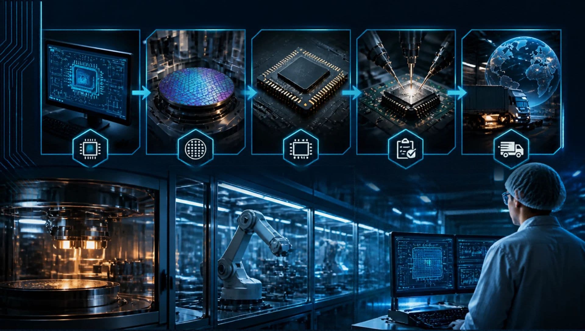
This feature offers a strategic lens on today’s semiconductor industry trends, designed especially for students and early-career professionals. We’ll explore the entire semiconductor value chain, from architecture design to customer qualification, delve into key technologies, highlight real workplace examples, and unpack how AI complements expert roles rather than replaces them. Our goal is to build your practical capability, helping you see the bigger picture while mastering the details that matter in your role.
Understanding Industry Trends: The Backbone of Semiconductor Innovation
The semiconductor industry is far more than churning out chips. It represents the strategic engine powering the digital economy—from smartphones to autonomous vehicles and cloud data centers. Trends in this sector ripple through the entire tech ecosystem, affecting how products are designed, manufactured, and delivered.
Some of the core industry trends include:
Advanced Node Shrinking and Chiplet Architectures: Progress in lithography allows feature sizes to shrink below 5 nanometers, but physical and economic limits are driving innovation towards chiplets modular chip components that can be integrated like building blocks. This improves yield economics and design flexibility.
Artificial Intelligence (AI) in Design and Manufacturing: AI-powered software aids defect analytics, predictive maintenance of fab equipment, and simulation-driven design verification, enhancing precision and reducing time-to-market without supplanting human expertise.
Digital Twins and Smart Fabs: Factories increasingly employ digital twins—virtual replicas of fabrication lines—to optimize yield and predict equipment downtime, driving collaboration among design, process, and equipment teams.
Advanced Packaging and Integration: Beyond traditional fabrication, packaging innovations such as 3D stacking and heterogeneous integration enable chips with higher performance and better energy efficiency.
Supply Chain Resilience: Events in recent years spotlighted the need for robust supply chain strategies, blending agility, digital tracking, and cross-company collaboration across the value chain.
Turning Trends into Workplace Insights: A Yield Loss Investigation Example
To see how these trends manifest on the shop floor, consider a yield loss investigation—a common but complex workplace challenge. Imagine the test engineers notice a sudden dip in yield during final testing, indicating that more chips than usual are failing to meet specifications.
With advances in metrology and AI-powered defect analytics, the process team collaborates closely with design verification and equipment groups. By leveraging digital twins of the production line, they simulate fab conditions and cross-reference data from EDA tools (Electronic Design Automation), seeking anomalies invisible to manual inspection.
AI-driven predictive maintenance tools flag recently serviced equipment as a potential root cause, while advanced packaging inspection sensors detect subtle bond failures. The teams confirm the issue stems from slight equipment misalignment during bonding, quickly realign machines, and restore yield to target levels.
This example illustrates how cross-functional collaboration, powered by industry trends like AI and digital twins, supports rapid problem-solving—preserving precision and reliability, core industry principles.
How Industry Trends Translate into Business Value
Why do semiconductor companies invest heavily in these trends? The answer lies in delivering measurable business value across several dimensions:
Yield Economics: Small improvements in yield directly boost revenue since fewer wafers or chips are scrapped. Existing equipment runs more efficiently, reducing costs.
Speed to Market: Faster verification cycles, rapid design iteration via AI simulations, and agile supply chains help companies launch products ahead of competitors, securing market share.
Customer Value: Advanced packaging and heterogeneous integration enable sophisticated chip capabilities, supporting innovative end products that drive customer satisfaction and loyalty.
Precision and Reliability: Defect analytics and predictive maintenance ensure product quality and manufacturing uptime, critical in a market where errors can delay entire product lines.
These value drivers emphasize why understanding and participating in trends is essential for everyone in the semiconductor ecosystem—not just executives or senior engineers.
The Role of AI: Augmenting, Not Replacing Expert Judgment
AI often generates excitement and concern alike. In semiconductors, it’s vital to appreciate AI’s supporting role rather than see it as a replacement. AI models analyze vast datasets—such as defect patterns, tester outputs, or fab sensor signals—identifying subtle correlations and predicting outcomes faster than humans alone.
Yet humans remain central:
Interpreting AI findings in the context of engineering judgment and domain expertise.
Designing experiments or verification plans informed by AI but adapted to changing product requirements.
Collaborating across teams to implement practical solutions guided by AI insights.
For example, in equipment maintenance, AI may forecast failures, but technicians must decide when and how to intervene, balancing cost and uptime priorities.
Recognizing this synergy supports a growth mindset—learning to use AI tools effectively becomes a career capability that complements foundational engineering and process skills.
A Practical Framework for Exploring Semiconductor Industry Trends
To organize your learning and career development, consider this framework aligned with the semiconductor value chain and emerging trends:
Value Chain Stage | Relevant Trends and Technologies | Skills to Develop | Workplace Example |
Architecture & Design | Chiplet modularity, AI-driven simulation, EDA tools | Digital design, simulation, scripting | Participating in design reviews |
Verification | AI-based verification, defect simulation | Test planning, data analysis | Verification plan refinement |
Fabrication | Lithography advances, smart fab digital twins | Process control, equipment knowledge | Yield loss investigation |
Packaging & Testing | Advanced packaging, 3D stacking, metrology | Failure analysis, quality control | Packaging defect root cause analysis |
Supply Chain & Customer | Supply chain resilience, customer qualification processes | Logistics understanding, communication | Coordinating supplier evaluation |
Use this matrix as a roadmap—assessing your current skills, identifying priority trends to study, and seeking opportunities at work to apply new knowledge.
What Should Early-Career Professionals Explore Next?
If you’ve absorbed the gist of semiconductor industry trends and their workplace relevance, a good next step is a deeper dive into AI’s practical applications in fabrication and yield analytics. Explore how defect classification algorithms work, or how digital twin simulations model specific fab processes.
Reflect on this question
How can I proactively engage with cross-functional teams to better understand and contribute to ongoing innovation across the value chain? Collaborative projects and mentorship will amplify your growth far beyond individual study, preparing you for a career not just defined by technical skills, but by strategic thinking and adaptive learning in one of today’s most dynamic industries.
Frequently Asked Questions
What are chiplets and why are they important in semiconductor design?
Chiplets are modular blocks of semiconductor functionality that can be combined to create a complete system on a chip (SoC). They offer flexibility for design customization and can improve manufacturing yield by isolating defect risks. This approach helps overcome physical scaling limits of traditional monolithic chips and supports heterogeneous integration of specialized functions.
How does AI support semiconductor manufacturing without replacing engineers?
AI helps by analyzing complex datasets such as defect patterns, equipment sensor signals, and simulation outcomes much faster than humans. It predicts equipment failures, classifies defects, and optimizes processes. However, engineers interpret AI results, make decisions on interventions, and design verification experiments, maintaining control over critical judgments.
What skills should I focus on to enter the semiconductor industry today?
Start with foundational knowledge in digital logic design, semiconductor physics, and basic fabrication concepts. Learn to use EDA tools and develop data analysis skills, including programming basics like Python. Understanding collaboration across design, verification, process, and test functions is key. Developing soft skills such as communication and problem-solving is equally important.
How can early-career professionals contribute to yield improvement efforts?
Engage in cross-functional teams investigating yield loss by learning to interpret test data and manufacturing metrics. Participate in root-cause analysis sessions and familiarize yourself with defect analytics tools and digital twin simulations. Asking questions and volunteering for small data-driven projects builds capability and visibility.
What role does supply chain management play in semiconductor manufacturing?
Supply chain management ensures the smooth flow of materials, equipment, and finished chips, affecting production schedules and delivery commitments. Resilient supply chains adapt to disruptions, leverage digital tracking, and foster collaboration with suppliers and customers, supporting overall business agility and speed to market.
What emerging trend in semiconductors should I explore after AI and chiplet architectures?
Digital twins and smart fabs represent a promising next step. These virtual simulations of physical manufacturing facilities allow process teams to predict equipment behavior, optimize runs, and assess yield scenarios without disrupting actual production. Understanding how digital twins integrate with process control systems will be valuable.
Tags
Share this article

Omnivance Research Team
Dedicated to bridging the gap between education and industry requirements.
Related Courses
Deepen your knowledge with these recommended courses